Core idea
Computers have always been designed around this idea of determinism - they follow instructions.
I have always like programming because it is deterministic. Real life is messy - everything behaves in interesting ways, but nothing is exact - almost every measurement has a tolerance. This is much unlike modern digital compute - everything is exact — and we invest significant effort into keeping it that way with error checking and correcting algorithms, complex design to prevent bit flips from EMI and crosstalk.
What if, instead of trying to eliminate noise, we used it?
The idea of probabilistic computing is that many processes are best modelled as a statistical distribution and we can solve difficult problems by creating a statistical model, and letting it “relax” to find an optimal solution.
The hardware primitive of this is called a “p-bit” (Probabilistic bit) - this fluctuates between 0 and 1 with a probability of each state defined by each of its neighbors and a “coupling” strength (similar to a weight in Neural Networks).
Wobbly Bits is my implementation of this on silicon. It has 6 p-bits (not very many…) on a real chip, with ring oscillators (a source of randomness) and some electronics to decide whether to flip the state of each p-bit.
How it works
The first problem that came to mind when designing this was: how do we create randomness.
Insane amounts of engineering effort is undertaken to make modern chips predictable. At the fundamental level they are representing mathematical equations that are consistent.
The answer is kinda cool - we use a ring of not gates to form an oscillator. If we have an odd number, there is no stable state for the circuit!

That solves the randomness part, but how do we actually work out the state of each P-bit?
I elected to use a “Round Robin” update cycle - we iterate over each p-bit and use this formula to decide its next state (J is the coupling matrix, i, j is the coordinate of the current pair):

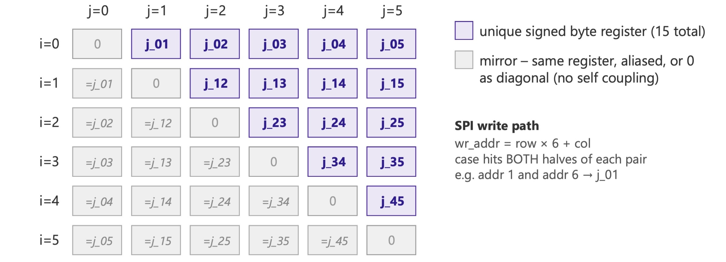
Here, s_j is the binary state of each neighbour (0 or 1), J[i][j] is the coupling strength between p-bits i and j — analogous to a weight in a neural network — and trng_byte is a random byte drawn from the ring oscillators:

thresh maps the net field linearly into a probability: net=0 gives 50/50 probability. Positive values bias toward 1; negative toward 0.
That is the core principle of how the device works.
Building it
When I dived into this project, I knew fairly little about how we can define hardware as code - all of my electronics experience so far has followed the same process - circuit design -> schematic capture (perhaps some simulation) -> manual layout and routing.
The first section of chip design is moving from a schematic to an HDL, such as Verilog. When I started, I immediately assumed that this was like a traditional programming language - the instructions you write get executed sequentially, perhaps with some jumps and loops to other parts of code.
I was very wrong — and that reframing was one of the most important things I learned on this project.
HDLs are quite different in the sense that they are much closer to a schematic than a programming language. They define connections between gates, not instructions (this is a bit of an oversimplification, but bear with me).
This was a tricky one to wrap my head around, as when I look at Verilog on a screen, my brain immediately assumes programming, however this is the wrong way to approach writing HDL.
To learn HDL, I took the NAND2Tetris Course, and thoroughly recommend it.
Once you have written some HDL and tested it (more on that later), you need to convert a group of logic gates to a design for a chip. This is much like the layout of a PCB, except it is mostly done automatically.
You have blocks (cells) that come from the chip manufacturer’s PDK (Process Design Kit). These are pre-validated silicon structures for different gates. My design uses many different types of cells (below), from NAND gates to buffers to inverters.
These cells are then wired up, however, at the modern chip scale, this is not possible by hand - Apples latest chip, the M5, contains ~28 Billion transistors. There is no way that a human, or group of humans could manually decide how to wire them up. Without spending a huge amount of time.
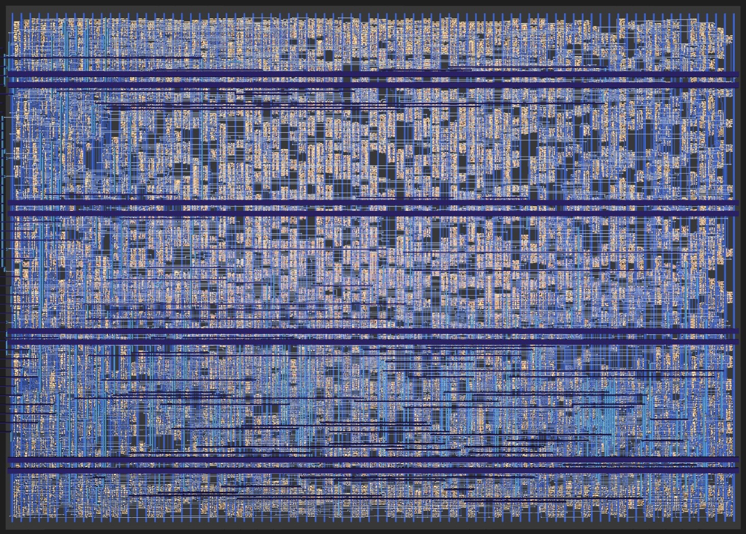
Luckily, computers are very good at optimisation problems. There is a great opensource workflow that lays out the chip by selecting where cells go and placing wires. This creates the 3D model you see below.
Testing
Silicon is expensive. It is also slow (~7 months from design to manufacture).
So despite considering myself totally infallible, I did write some testbenches for this.
This is much like a traditional testbench for software - you setup the chip in some way, and simulate the logic you have written to make sure the chip does something sensible.
The other form of testing is Gate Level testing. This is much more computationally intense and sort of akin to SPICE simulation of a circuit - here you simulate the actual gates used rather than the logic in the RTL.
The most interesting test that I did was to simulate solving a MAX-CUT problem (on a 3x3 matrix) on my chip. In simulation, we find that 44.5% of samples are “ground-state” or optimal solutions, against a 3.1% random baseline. This is clear if you look at the distribution of samples (read the docs for this project for more info)
Great, but is it useful?
In short: no.
Six p-bits cannot really solve any meaningful problems, but it’s an interesting proof-of-concept, and in some senses is quite scalable - I chose 6 as it was the maximum amount I could fit on the area that I can get through a 1x2 tiny tapeout tile, but there is no reason why we could not make a larger chip.
What I’d change
Six p-bits is enough to demonstrate the concept, but not enough to do anything really interesting. Real optimisation problems need hundreds to thousands of p-bits to work. The main constraint was tile area on the Tiny Tapeout shuttle; scaling up means a larger tile or a different process (I’m considering making it at the PCB scale as I can iterate much quicker that way).
The round-robin update scheme — one p-bit updated per clock cycle — is also an oversimplification. A true Gibbs sampler would update all bits in parallel, which would change the behavior, and make it converge faster. Doing that properly requires multiple independent entropy sources, and three ring oscillators isn’t quite enough for six simultaneous uncorrelated updates.
Moving forward I want to explore a PCB-scale version where I can iterate much faster — and scale to the hundreds of p-bits needed to tackle problems that are more interesting.